Quick contact →
- Tel.: +420 736 291 829
- E-mail: info@speltronic.cz
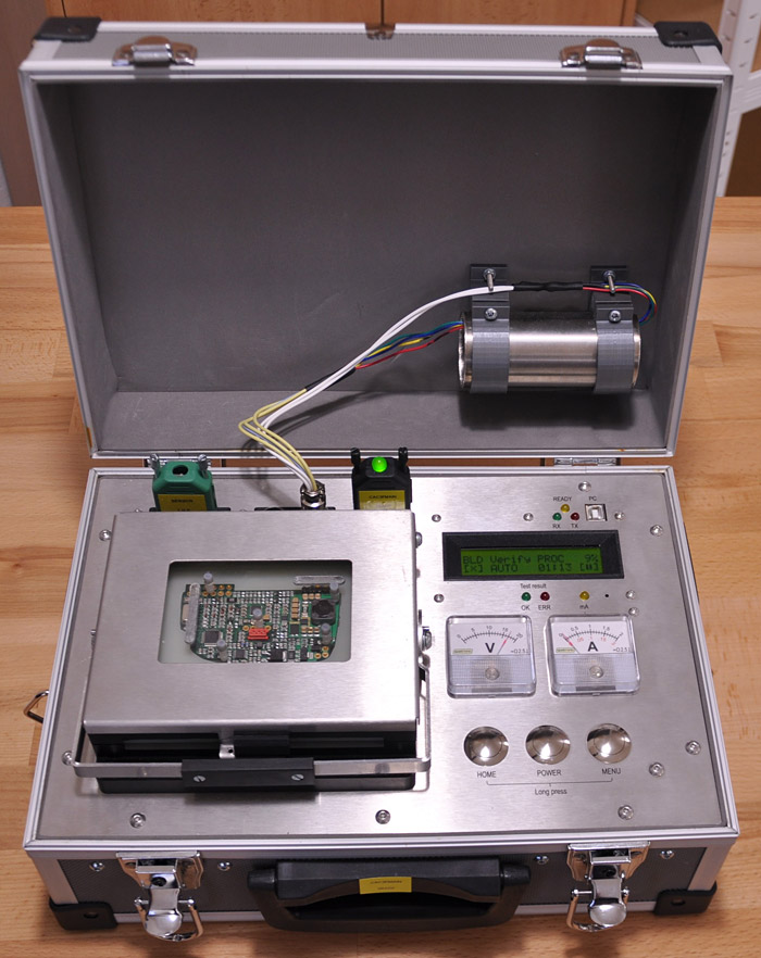
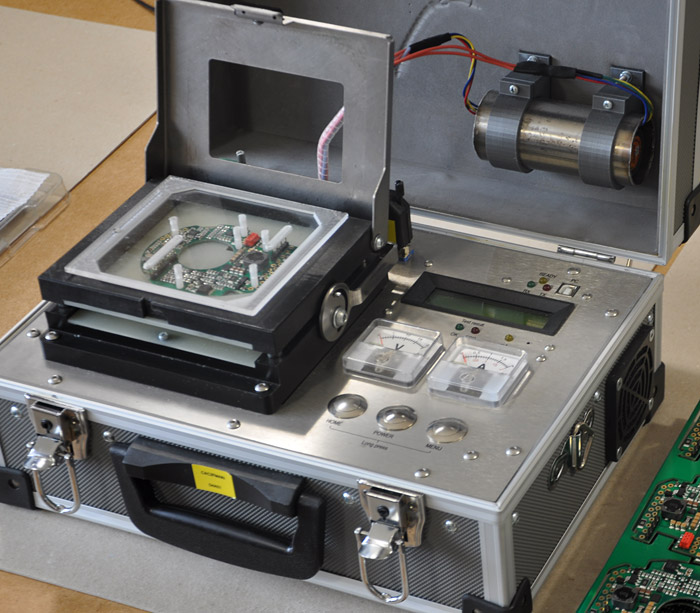
 The Speltester developed by our company is a comprehensive device for automatic commissioning and testing of printed circuit boards (PCBs). It was originally designed to streamline our own production. Over time, however, new features were continually added and the development environment for producing test programs was improved, making the tester a universally usable test device.
The PCB under test is inserted into a special matrix that connects the test points on the PCB to the tester electronics via flexible needle contacts. In this way, the PCB can be easily tested without the need to connect cables with connectors. The user then runs the test program on the tester.
The Speltester is a stand-alone device and does not require a PC connection for normal operation. Connection of the tester is only necessary for debugging test procedures, uploading procedures to the internal memory of the tester, updating firmware, etc.
The tester is designed so that it does not require a highly skilled operator in normal use. Access to the tester menu is restricted by a password and the test procedure selection is simplified by the use of a HW key. Thus, each type of PCB under test can have its own HW key, which, when inserted into the tester, ensures correct configuration.
Testing with this tester has resulted in significant production efficiencies compared to manual recovery and testing. A typical recovery and functional test of a single PCB with an ATMega328 processor, including bootloader upload and verification via ISP, application bootloader upload and verification via serial link, and operator intervention associated with inserting and removing the PCB from the test die takes approximately 3-5 minutes. Further efficiency gains are possible by running multiple testers in parallel, one worker can easily handle multiple testers.
